

Multi-Band Antenna Matching
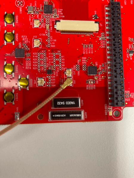
We brought all four ISM bands on a TI CC1101-based transceiver under the −10 dB return-loss target, verified in the hardest condition to hit: fully assembled in its case with the display installed. A streamlined calibration method got us there in about six solder iterations per band, roughly half of what the textbook approach would have taken.
Project at a glance
| Bands matched | 4 of 4 in spec (315, 433, 868, 915 MHz) |
| Return loss | ≤ −10 dB across every band |
| Total coverage | 315–928 MHz |
| Iterations | ~6 solder iterations per band (about a 2× reduction) |
| Verification | In-case, with the display installed |
The Challenge
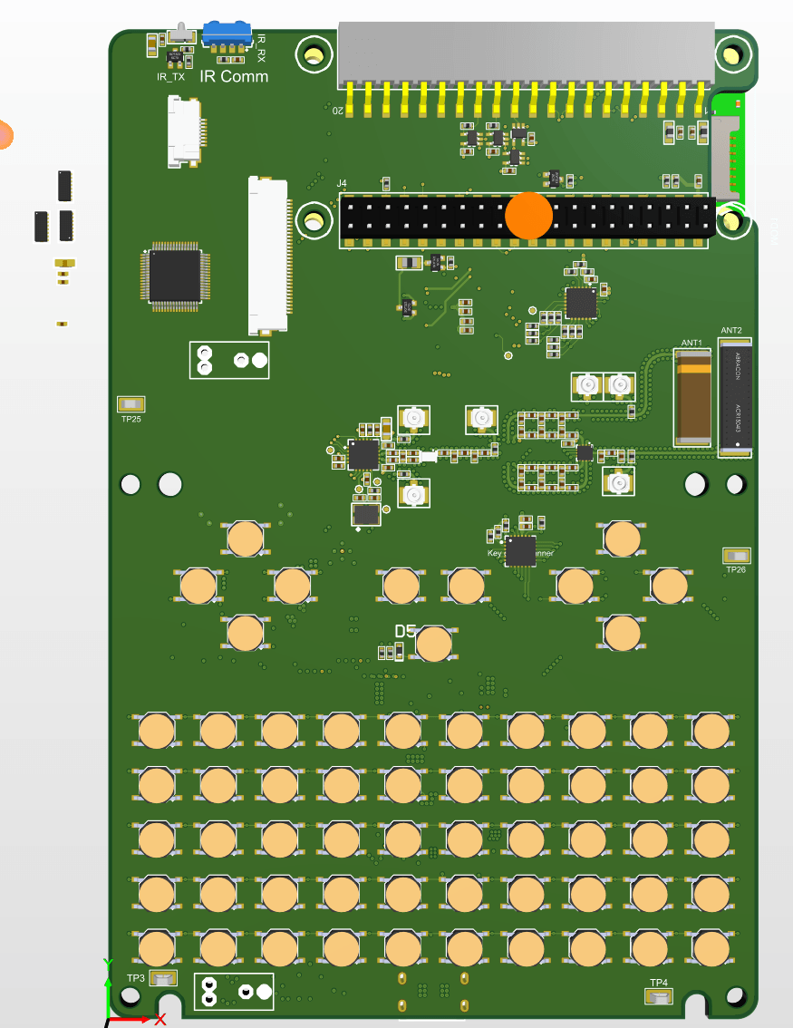
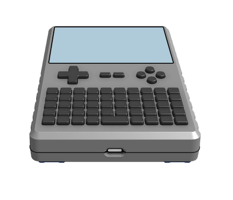
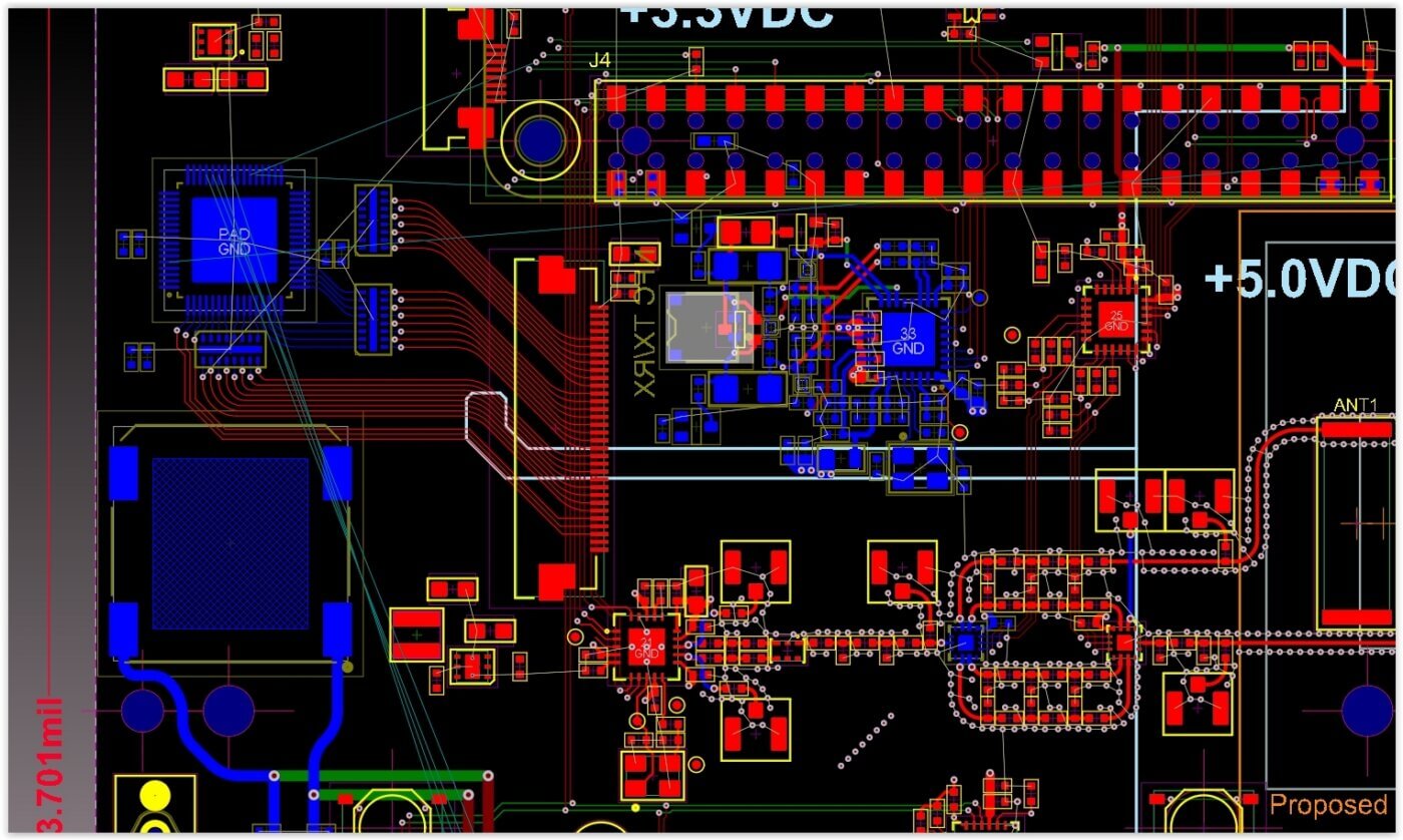
The product was a sub-GHz multi-band RF transceiver built around the TI CC1101. Four ISM bands routed through a single SP4T switch to two chip antennas that shared one corner of the board, with only one band active at any moment: a narrowband antenna for 315 MHz and a multi-band antenna covering 433, 868, and 915 MHz. Every band needed a matching network holding return loss at or below −10 dB across its operational range. A matching network tunes the electrical path between the radio and its antenna so power transfers efficiently instead of reflecting back, and return loss measures how much reflects. At −10 dB, only a small fraction returns, which is the practical threshold for reliable range and battery life on most sub-GHz radios.
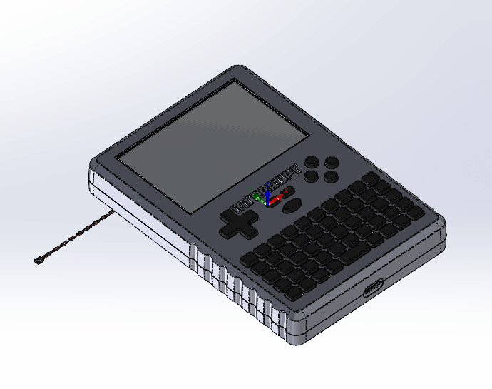
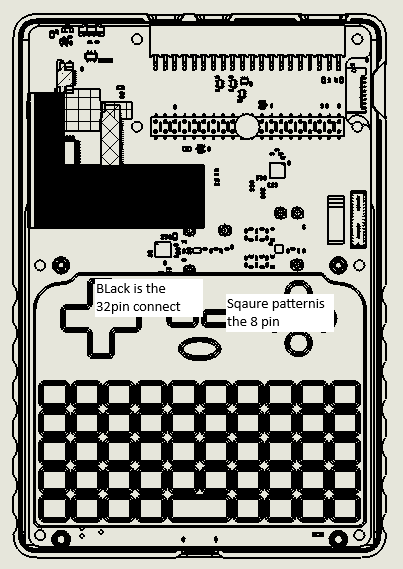
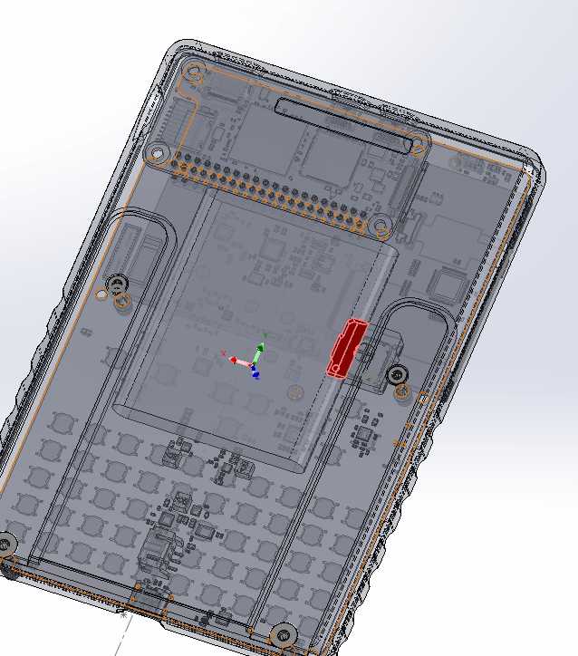
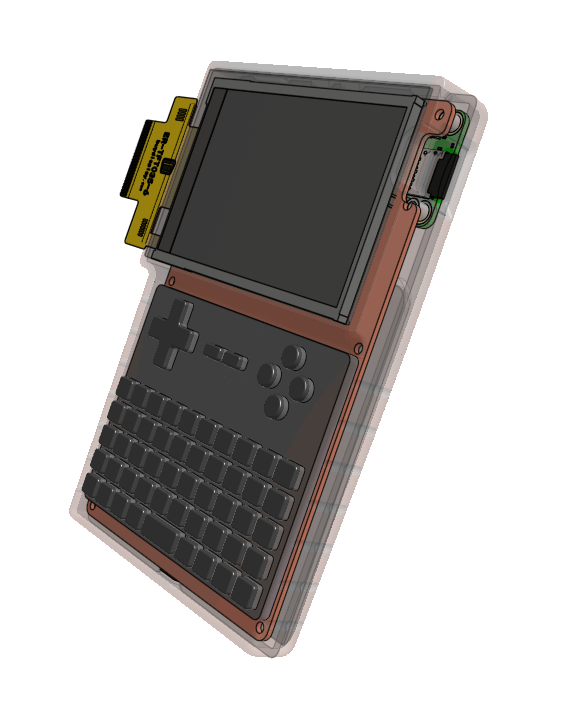
Two things made that harder than a single-band match. First, the spec had to be met in-case with the display installed, because the display is the closest metallic object to the antennas and the largest source of detuning. Matching on a bare board would have looked clean and failed in the real product. Second, the two antennas sat close enough to couple to each other, so tuning one band shifted the response of the others. Matching one band is routine RF work. Matching four coupled bands to spec inside the finished enclosure is where the difficulty lies.
The Solution
Kickr led the product development and paired one of our electrical engineers with specialist RF support from Marietta Research Solutions for this phase. That is the balance we aim for on every build: deep expertise applied exactly where a project needs it, without standing up a dedicated RF lab for a single stage of work. Agility and expertise are not a trade-off here. They are the point.
The team worked through three approaches before landing on the efficient one. A simple analytic model of the board was fast but could not converge without also capturing the balun and switch. A full short/open/load calibration was highly accurate but expensive to run, roughly a dozen calibration solderings per band plus additional components on every tweak. Sustainable for one band, not for four, given the board’s finite rework budget.
The method that worked was a three-measurement calibration: measure the antenna alone, then in series with a known inductor, then with an added shunt capacitor. Those three points are enough to extract the delay and attenuation of a simple model, after which two to three component iterations center each band. That came out to about six solder iterations per band, close to half the count a full calibration would have required across all four. On a board you can only rework so many times; that difference is the difference between finishing and starting over.
Order mattered too. Because the antennas coupled, the team tuned 315 MHz first, since shifts there propagated into the other three bands through the shared geometry. From there, 433, 868, and 915 MHz were remeasured, adjusted, and finalized in sequence.
The Results
All four bands passed; every measurement was taken in-case with the display installed.
| Band | Frequency range | Matching network | Measured return loss (in-band) |
| 315 MHz | 314–316 MHz (FCC Part 15) | 51 nH series, 7 pF shunt | −14 to −15 dB |
| 433 MHz | 432–434 MHz (Region 1 ISM) | 20 nH series, 0.5 pF shunt | −13.3 dB |
| 868 MHz | 863–870 MHz (ETSI EN 300 220) | 4 pF shunt, 15 nH series, 1.0 pF shunt | −15 dB or better |
| 915 MHz | 900–928 MHz (FCC Part 15.247) | 2 pF shunt, 15 nH series, 0.2 pF shunt | −17 dB at 911 MHz |
The 868 MHz band was the toughest of the four. A simple L-section could not pull the resonance far enough, so the team added a shunt capacitor to move it into band. The 915 MHz band carried the widest fractional bandwidth and still landed at −17 dB. The 433 MHz band scaled cleanly from the topology used elsewhere and needed no final tweak once 315 MHz was retuned.
Two recommendations went back with the design for the move to production. Verify the solution on a second fabricated board, since PCB-to-PCB variation in the balun, switch, and trace geometry is small but real. And specify 1–2% tolerance components for the tighter matches, because 5% parts can drift the resonance out of band. Getting a product to spec is the milestone. Making sure it stays there across a production run is the job.
RF engineering for the antenna-matching phase was performed in collaboration with Marietta Research Solutions, and published with their permission. A companion version of this case study appears on the MRS site.
Let’s bring your project to life
Big ideas deserve to make it to market. Whether your product needs RF engineering, firmware, industrial design, or all of it under one roof, our team of engineers is here to help. We offer free consultations and estimates.